
| |

|
|
|
Silicon Investigations Integrated Circuit Failure Analysis Services Overview:
There are four main phases of every IC failure analysis project. The first phase is non-destructive testing, where tools like parametric testing and x-ray imaging are applied to learn as much about the sample without permanently altering it in any way. Next comes fault verification, where we attempt to replicate the failing conditions reported by the customer; without confirming the failure, the project cannot continue, since there is no evidence to show that a defect even exists. With the fault confirmed, the next phase is fault isolation, where we identify a site for an in-depth destructive physical analysis and examination. We might use tools like voltage contrast scanning electron microscope images, laser induced voltage alteration (LIVA), or thermal imaging to locate a defect. In other cases, microprobing of the die or a careful optical or scanning electron microscope inspection of the die bonds might be sufficient to identify the root cause of failure. Contamination of the semiconductor surface and of the wire bonds can be analyzed using an EDAX x-ray detector on our SEM to identify the composition of the contamination. Finally, destructive analysis serves as the
culmination of all the data collection thus far: armed with the results
from fault isolation testing, we will perform deprocessing, a
cross-section, or other destructive technique to reveal the defect in
its entirety and identify its most likely cause. Destructive Analysis:
For integrated circuits, the first step is to access the silicon (or other semiconductor) die by removing or cutting a hole in the epoxy case, exposing the die. For epoxy encapsulated packages, this is accomplished by the use of strong acids and heat to dissolve the epoxy resin. For metal/ceramic packages, the package lid can be removed by heat or by shearing the ceramic at the seal line. 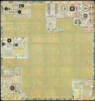
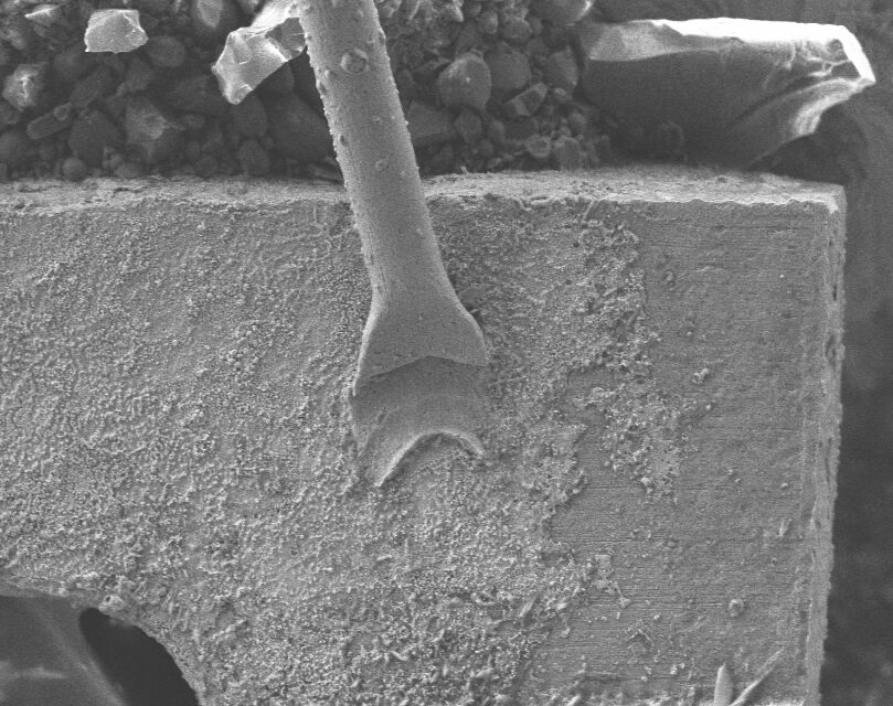
Shown to the right is a die removed from a wifi appliance. The packaging in this case was wafer scale with solder bumping. The polyimide coating on the bottom of the die was removed by plasma ashing in an oxygen plasma. The next step depends on the nature of the failure. If a failure of the wire bonds is suspected, we examine the bonds using optical and scanning electron microscope inspection equipment. This can reveal cracking in the wire bonds, bonding pad delamination, corrosion of the wire bonds due to chemical residues from the epoxy case or other sources, and thermal shearing of the wire bond. Below is an example of a copper wire bond that cracked due to poor material and annealing. The image is from our scanning electron microscope. 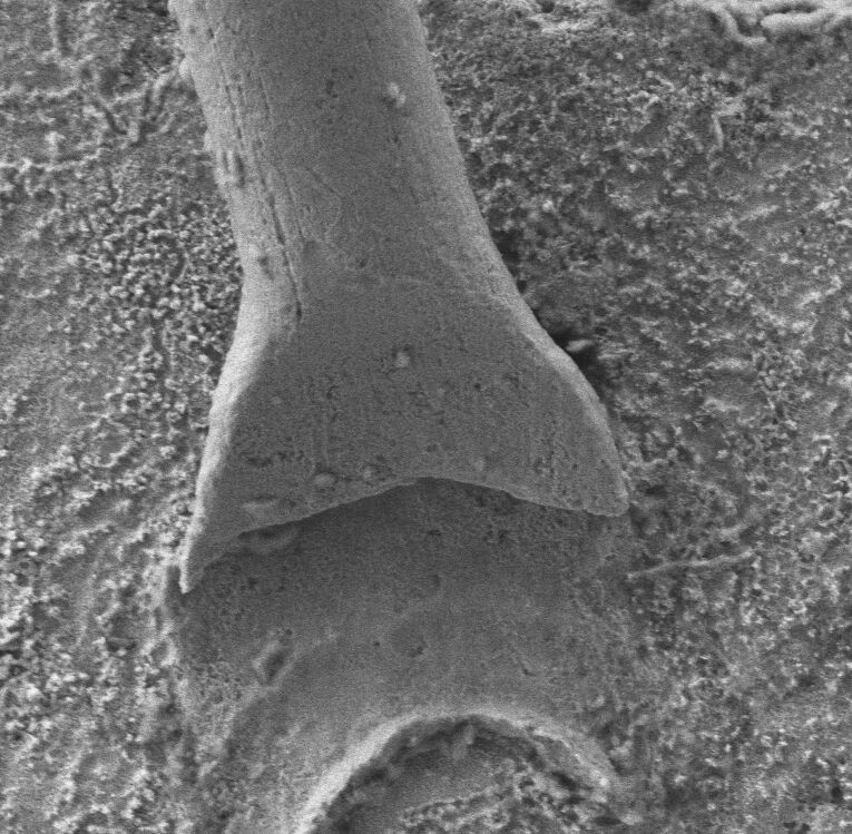
If electrostatic discharge damage is suspected, we can image the chip surface with a scanning electron microscope to locate the area of damage and determine the magnitude of the discharge that caused the failure. The images below show a gallium arsenide (GaAs) chip that was severely damaged by an electrical arc. As you can see, the gold metallization was not only vaporized, but the magnetude of the resulting plasma ablated the surface of the die. The Right image is of the full die. 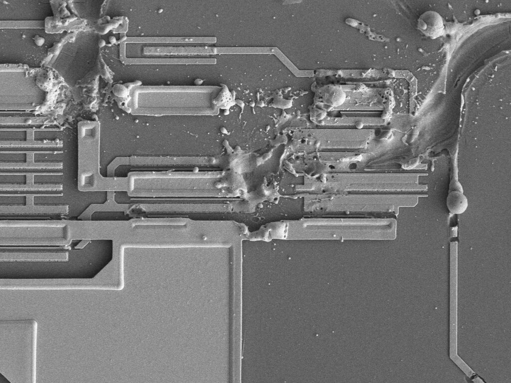
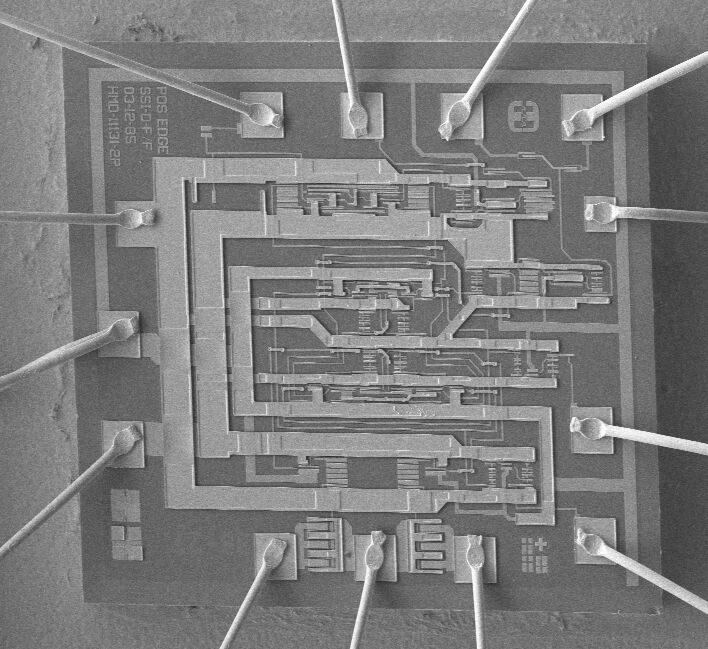
The below image is of a wire bond with a failure (delamination) of the connecting trace on a GaAs die. The failure is center bottom trace connected to the left wire bond. 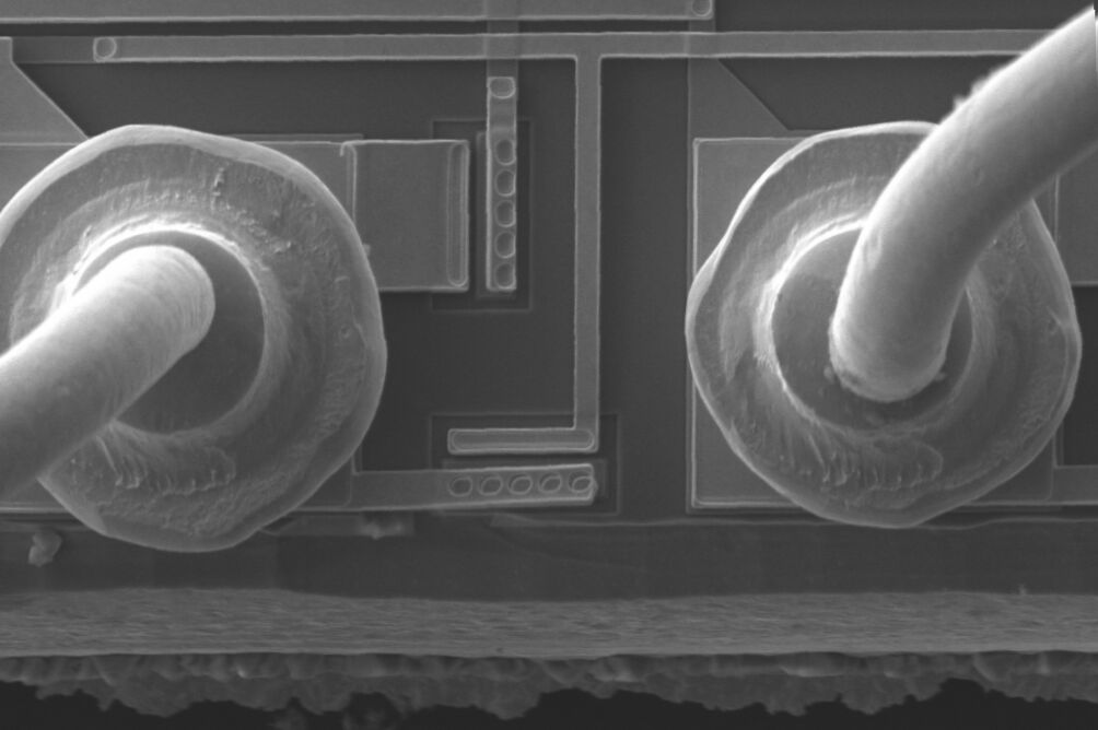
For a size comparison, the following image are grains of pollen stuck to one of the wire bonds on the above chip. 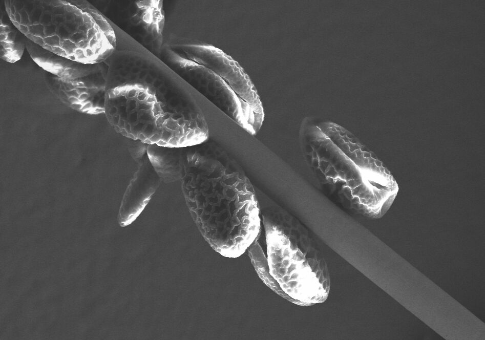
If the nature of the failure is such that it causes the chip to malfunction in an indeterminate way, such as an occasional latch up, we can use our SEM in voltage contrast mode, which allows us to map the charge on the surface of the chip, highlighting areas that are at a different electrical potential from the surrounding strucrures. Using this technique, it is possible to 'watch' the chip as it is given electrical stimuli at a low frequency, preferably by single stepping the logic. This allows us to view the chip in operation to detect the cause of latchup or otherwise undesirable operation. For further information, please don't hesitate to contact us. |
|
| |
Last Modified
May 29, 2020
This page, and all contents, are Copyright © 2004-2019 Silicon Investigations, Ltd. Appleton, Wisconsin, USA. |
|